Washington State University
Institute of Materials Research
Advancing materials discovery through crystal growth, microfabrication, and advanced characterization.
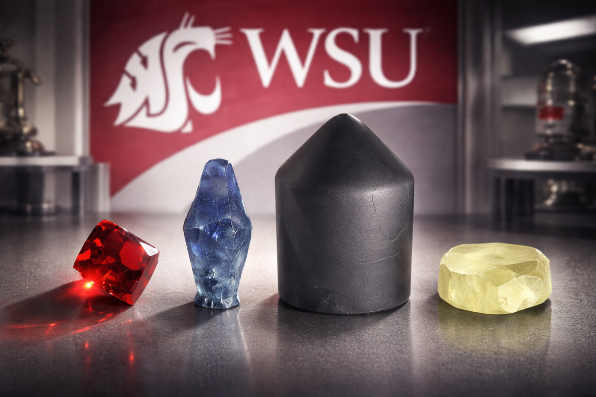
Crystal Growth
Engineering Advanced Crystals
Growth of high-purity semiconductor and oxide single crystals including CdTe, CdZnTe, Ga₂O₃, ZnTe, and laser materials such as ruby and sapphire.
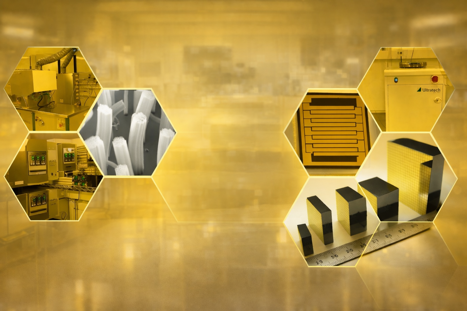
Micro / Nanofabrication
Cleanroom Device Fabrication
Micro- and nanoscale device fabrication in WSU’s
Class 1000 cleanroom facility.
Class 1000 cleanroom facility.
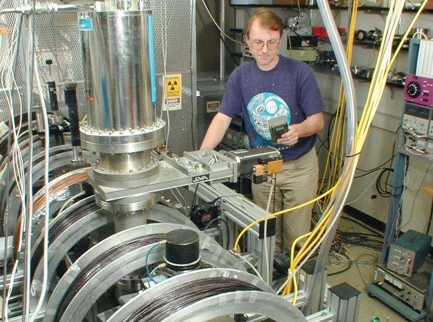
Advanced Characterization
Positron Annihilation Spectroscopy
A highly sensitive technique used to detect and analyze vacancy-type defects in materials at the atomic scale.
Advanced Characterization
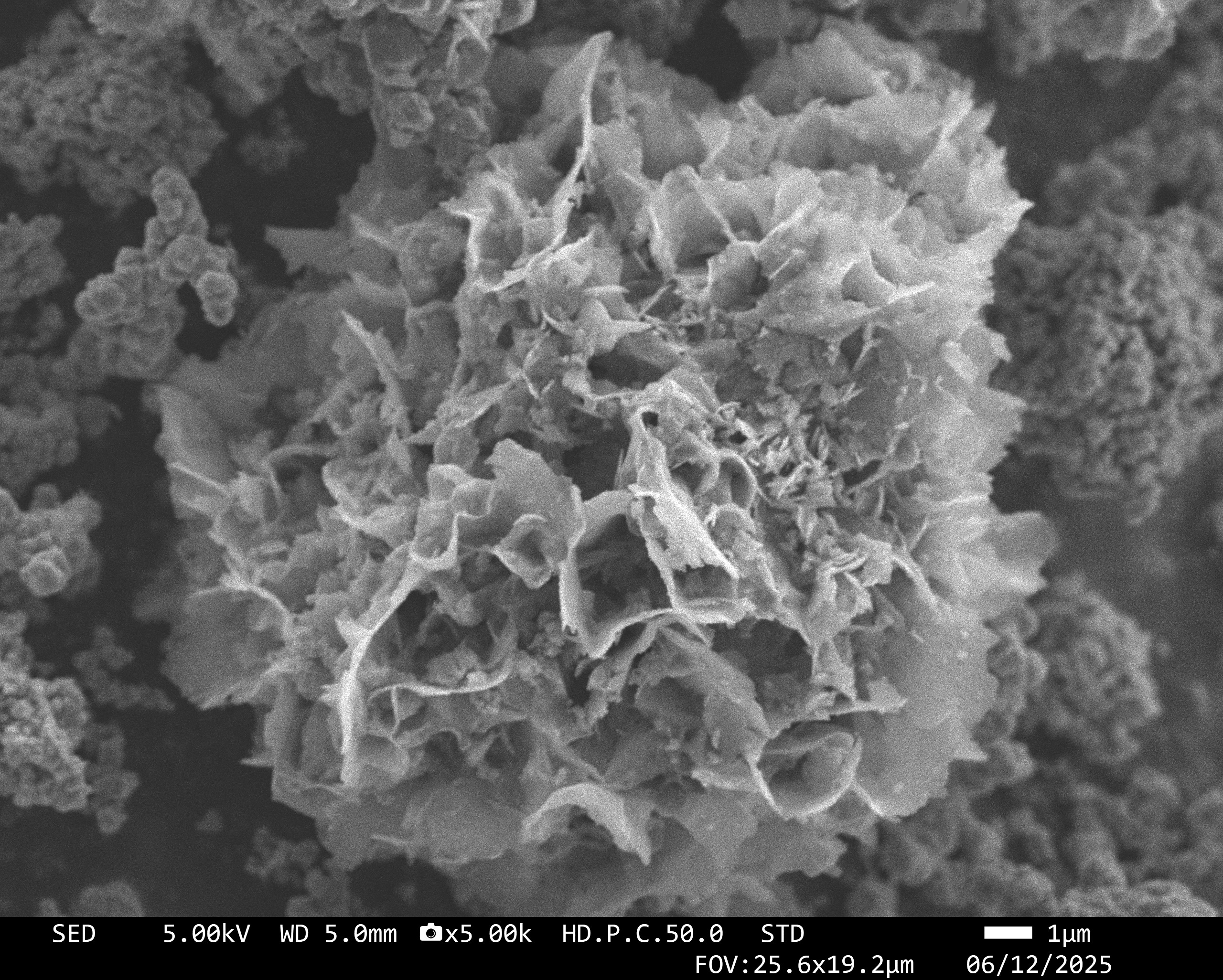
Scanning Electron Microscopy
JEOL JSM-IT800HL SEM: High-resolution imaging and multimodal analysis of materials using SE, BSE, TED, EDS, EBSD, and cathodoluminescence detectors.
Advanced Characterization
Nano-CT 3D X-ray Microscopy
Used to investigate pores, cracks, inclusions, and internal architectures in materials through non-destructive 3D imaging.
Established in 1993, WSU’s Institute of Materials Research advances interdisciplinary materials research, education, and innovation.
Featured Research
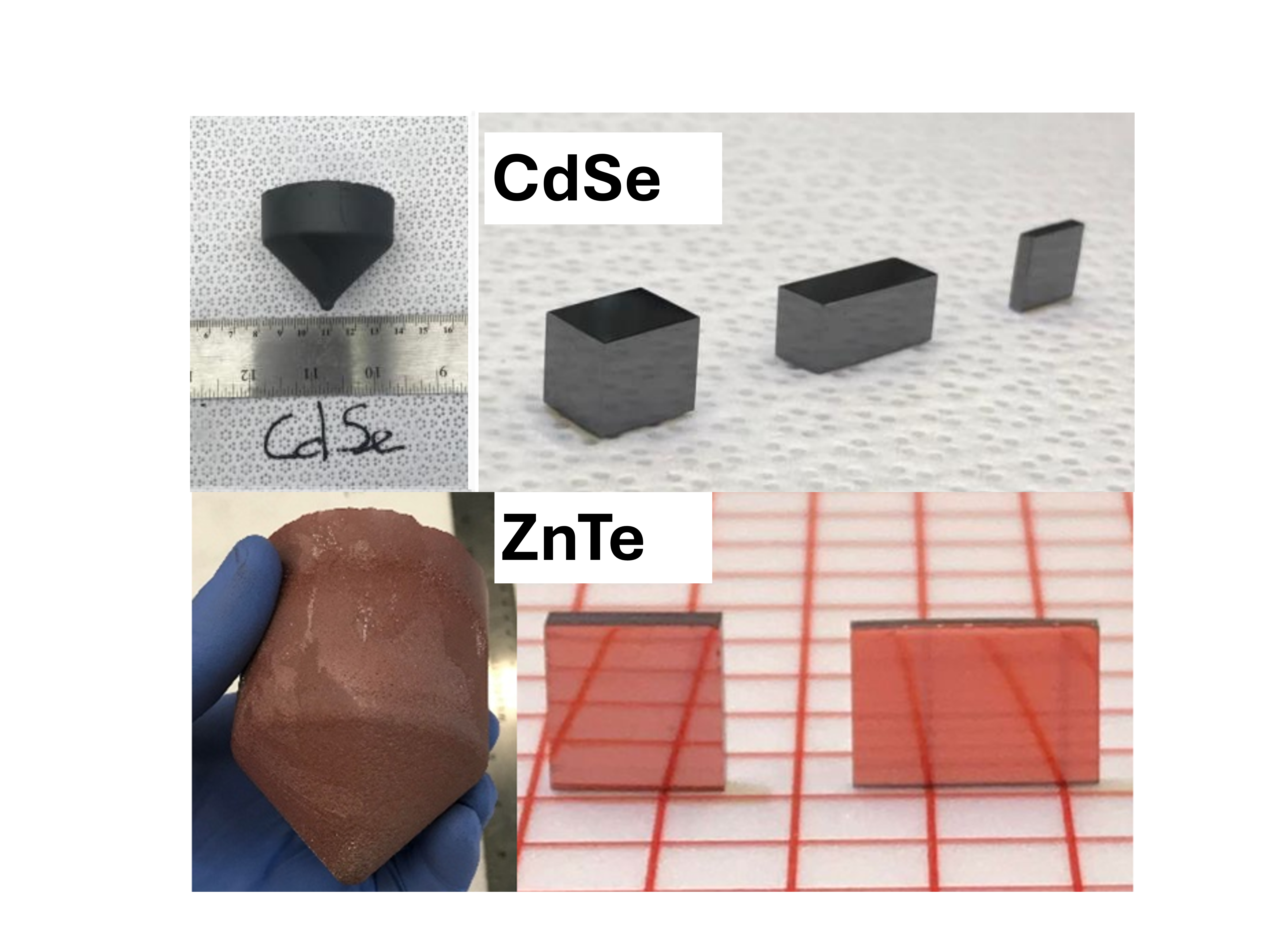
Infrared Optical Materials
Infrared optical materials and semiconductors, including ZnSe, ZnTe, CdSe, PbSe, CdTe, and related II–VI chalcogenides, for windows, imaging, sensing, terahertz, and photonic applications.
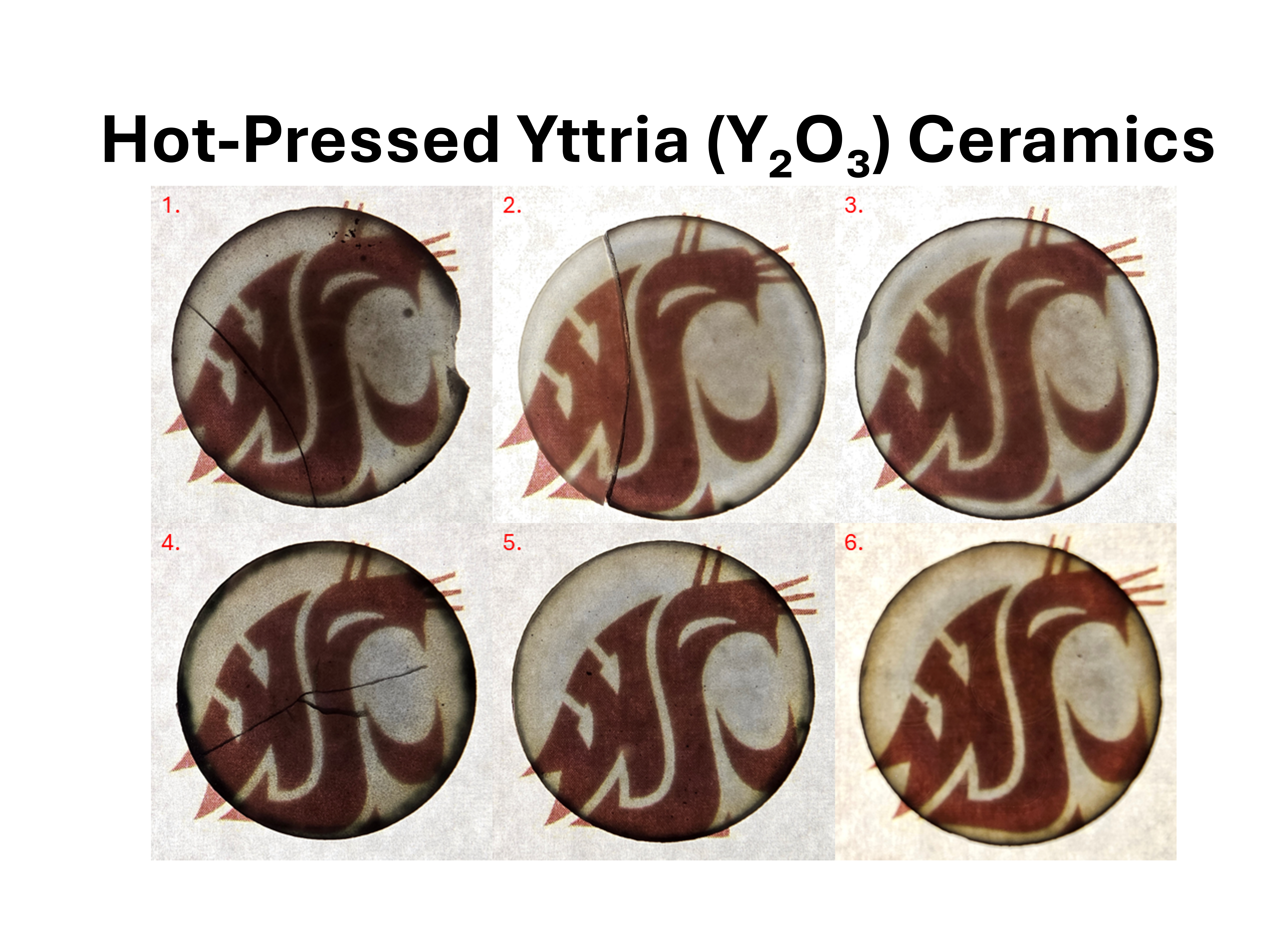
Transparent Ceramics
Transparent ceramics for infrared windows, lasers, imaging systems, and extreme-environment optical applications, such as Yttri(Y₂O₃).
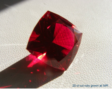
Laser & Optical Crystals
Ruby, sapphire, and functional single crystals for lasers, optics, sensing, and harsh environments.
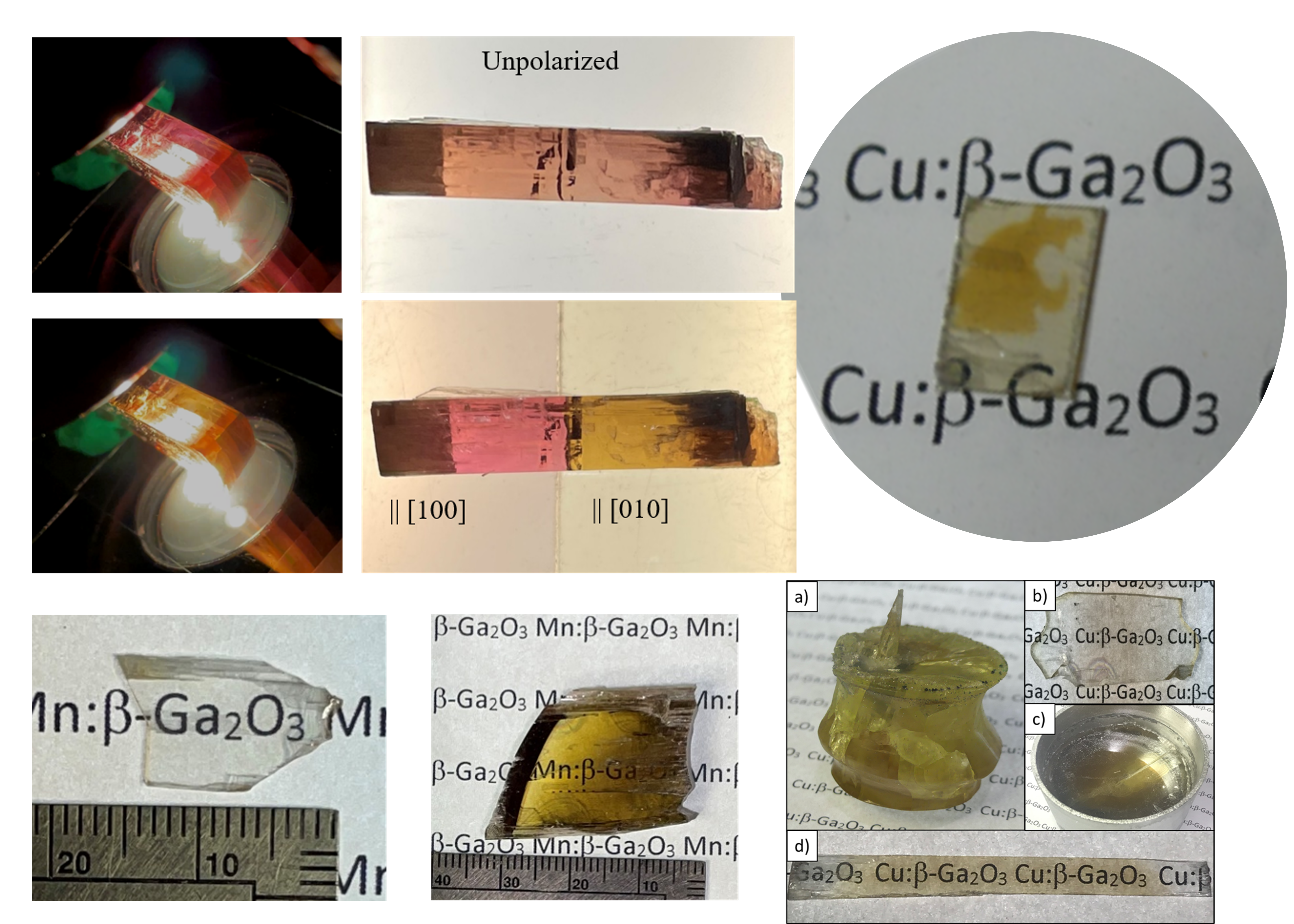
Ultra-Wide Bandgap Semiconductors
Crystal growth, defect engineering, and characterization of Ga₂O₃ and other ultrawide bandgap semiconductors for high-power electronics and deep-UV devices.
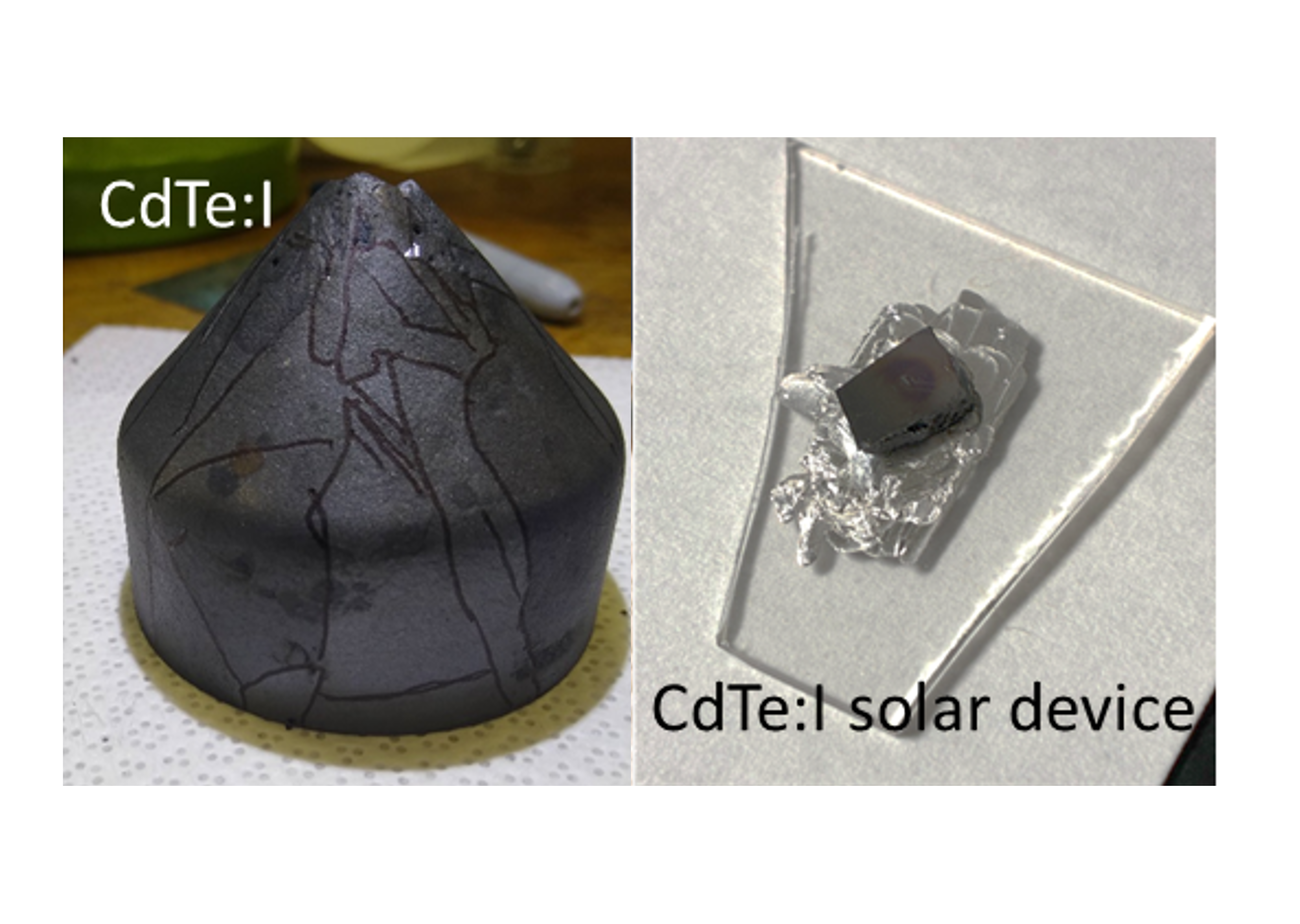
Renewable Energy Materials
High-performance semiconductor materials for next-generation photovoltaics, including CdTe and CdSeTe crystal growth, doping, and defect engineering.

Radiation Detection Materials
High-resolution CdZnTe detectors for medical imaging, homeland security, and nuclear safeguards.
Core Capabilities and Facilities
Crystal Growth
State-of-the-art crystal growth capabilities for semiconductors, optical crystals, transparent ceramics, and functional materials using CZ, HPB, Bridgman, THM, VGF, and related techniques.
Microfabrication
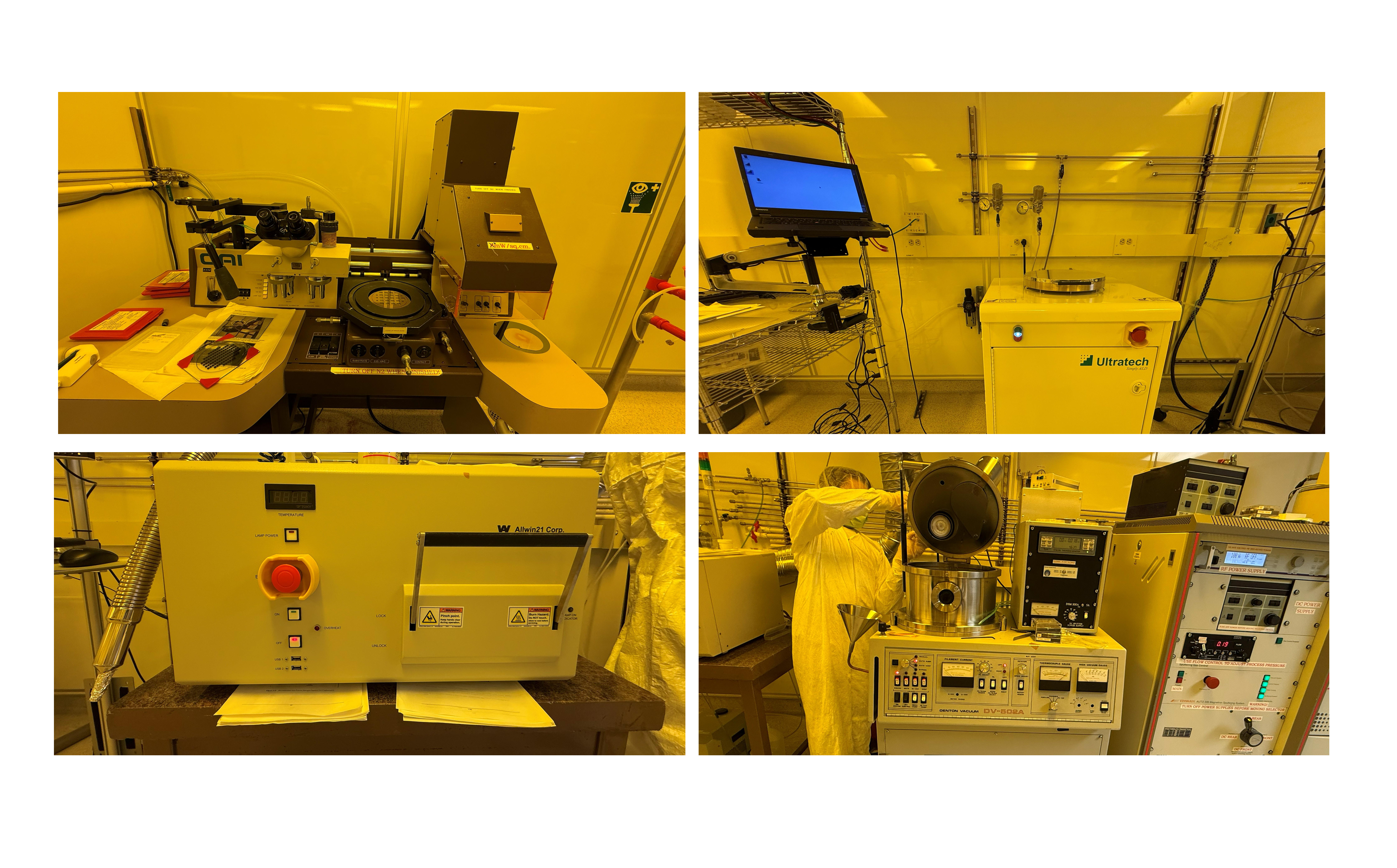
State-of-the-art cleanroom facilities for microfabrication, including photolithography, PVD and ALD thin-film deposition, thermal oxidation, diffusion, wet and dry etching, metallization, and device processing.
Glass Science & Engineering
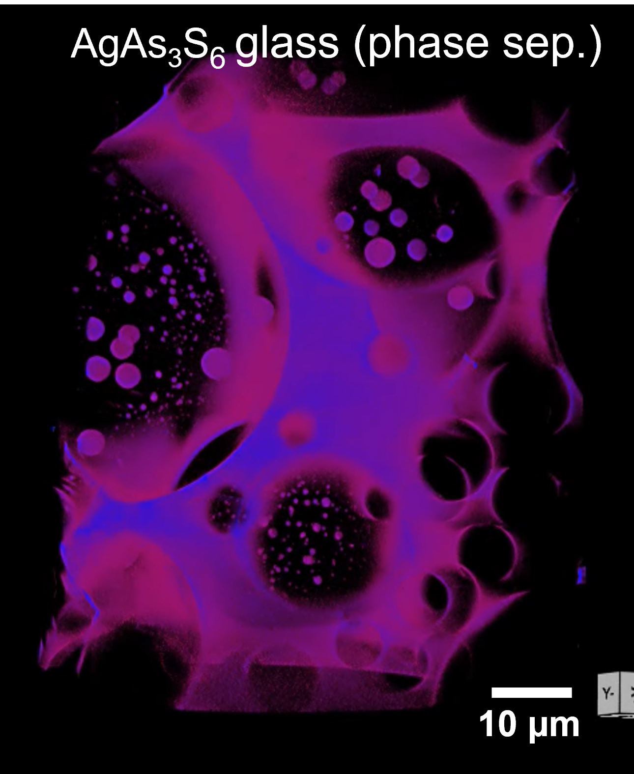
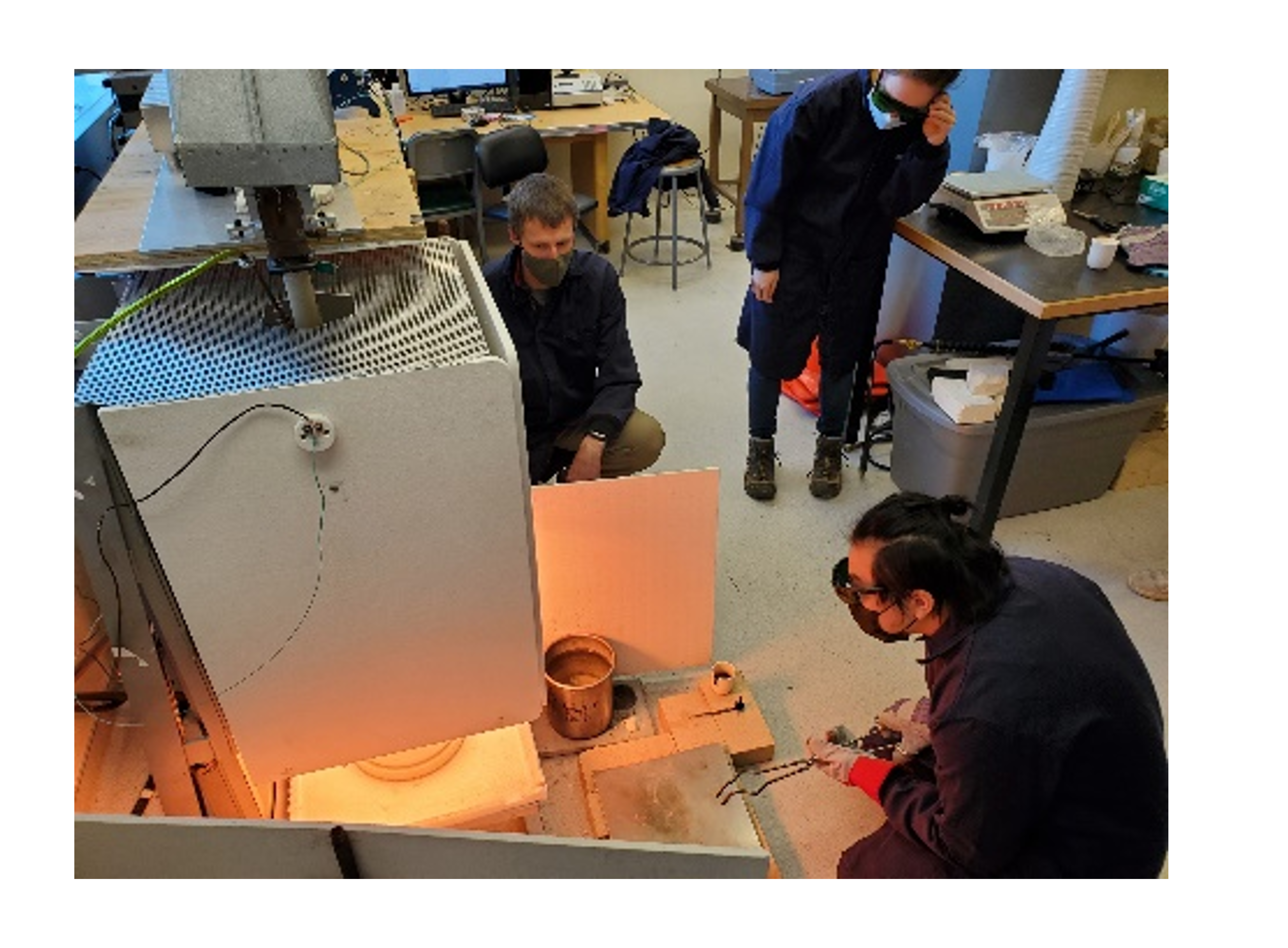
Glass melting, synthesis, heat treatment, and thermophysical characterization for optical, nuclear, and functional glass materials.
Ceramic Processing & Synthesis
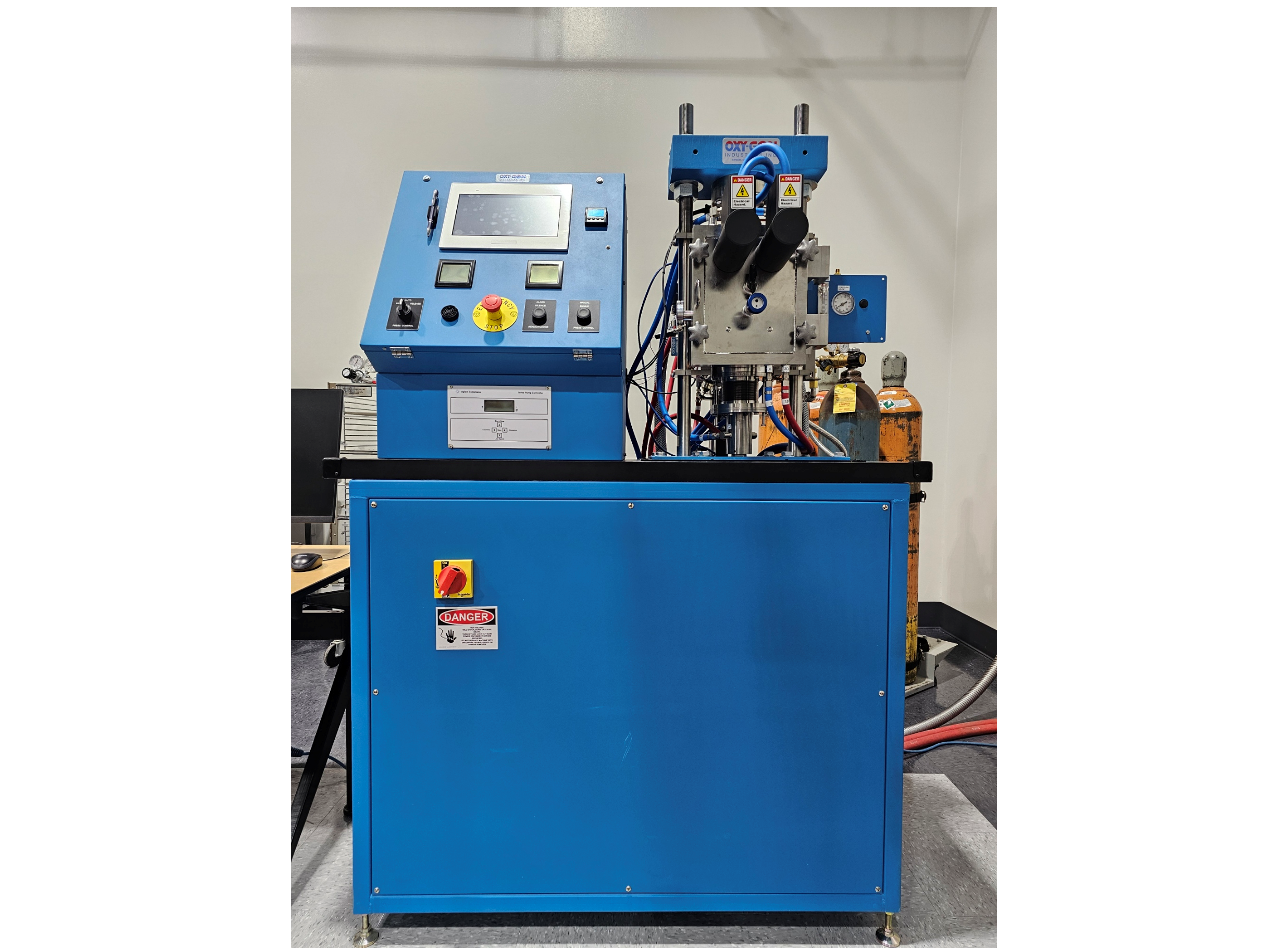
Advanced ceramic processing using hot pressing, pressureless sintering, controlled-atmosphere furnaces, and hydrothermal synthesis for structural and transparent ceramics.
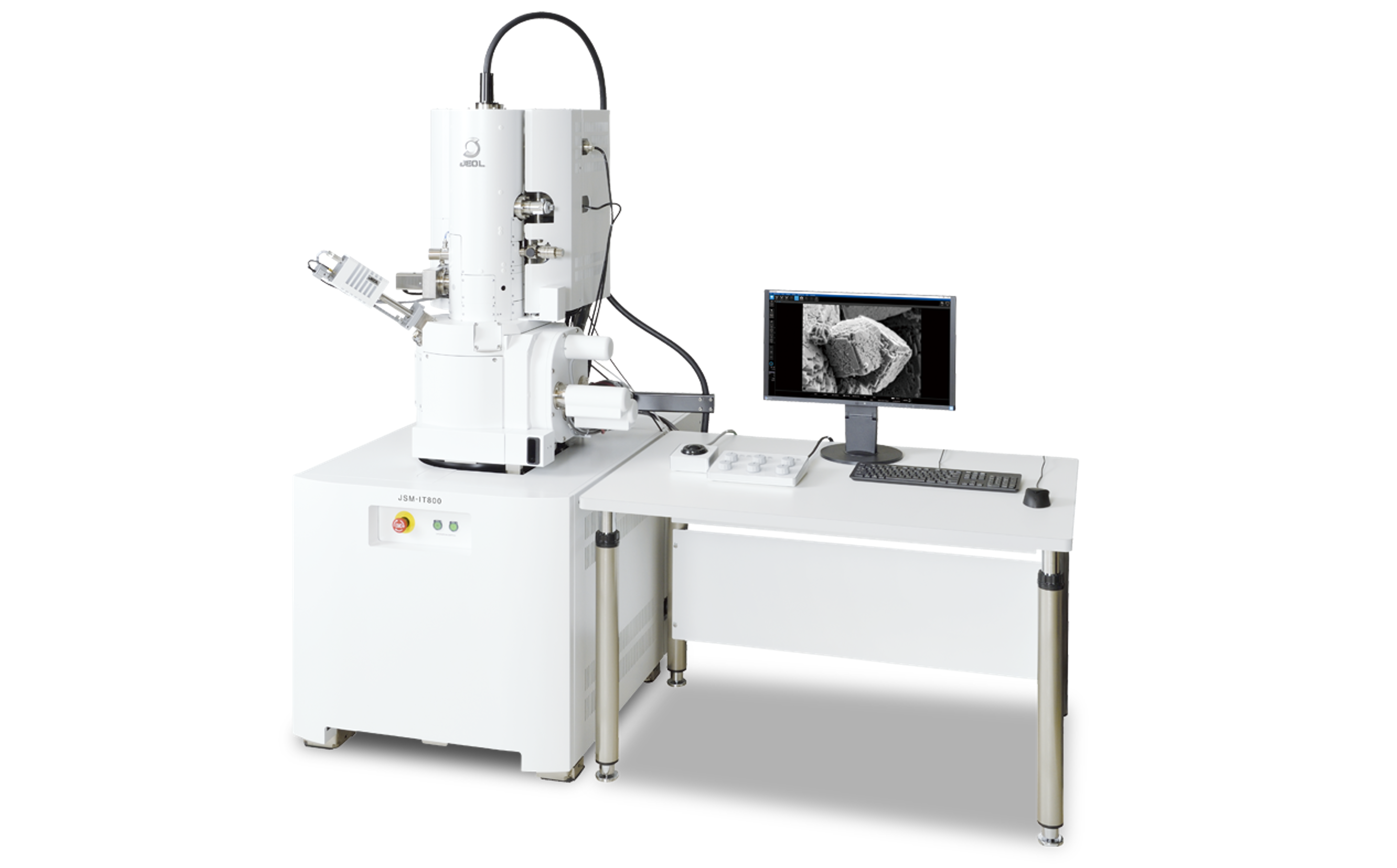
Scanning Electron Microscope
High-resolution imaging and microstructural characterization using the JEOL JSM-IT800HL field-emission scanning electron microscope (SEM), equipped with secondary electron (SE), backscattered electron (BSE), energy-dispersive X-ray spectroscopy (EDS), electron backscatter diffraction (EBSD), cathodoluminescence (CL), and transmission electron detection (TED) for morphology, composition, crystallography, and optical analysis.
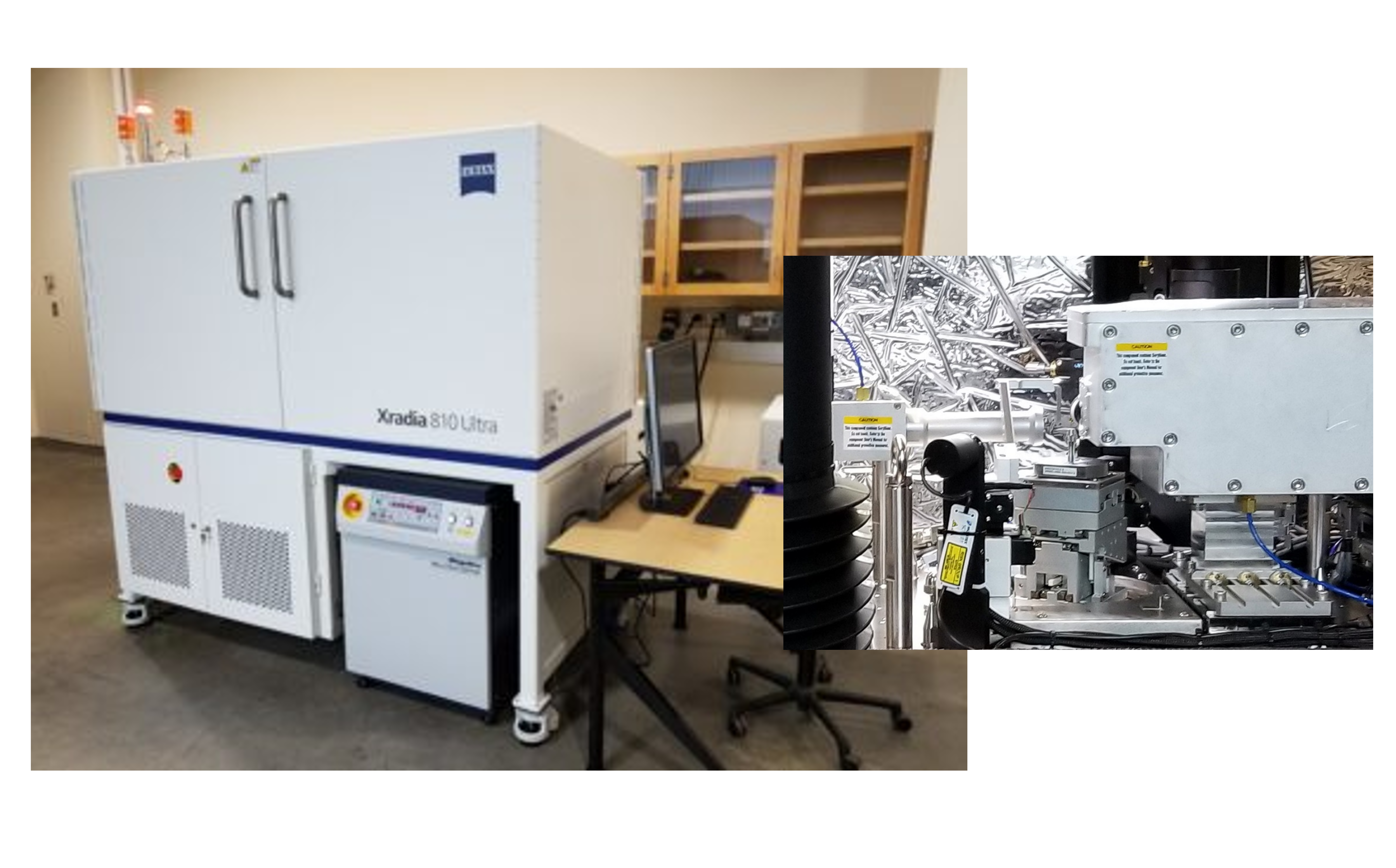
3D Imaging
High-resolution, non-destructive three-dimensional imaging using the ZEISS Xradia 810 Ultra X-ray microscope (nano-CT), enabling nanoscale visualization of internal microstructures, pores, cracks, inclusions, interfaces, and defects without destructive sample preparation.
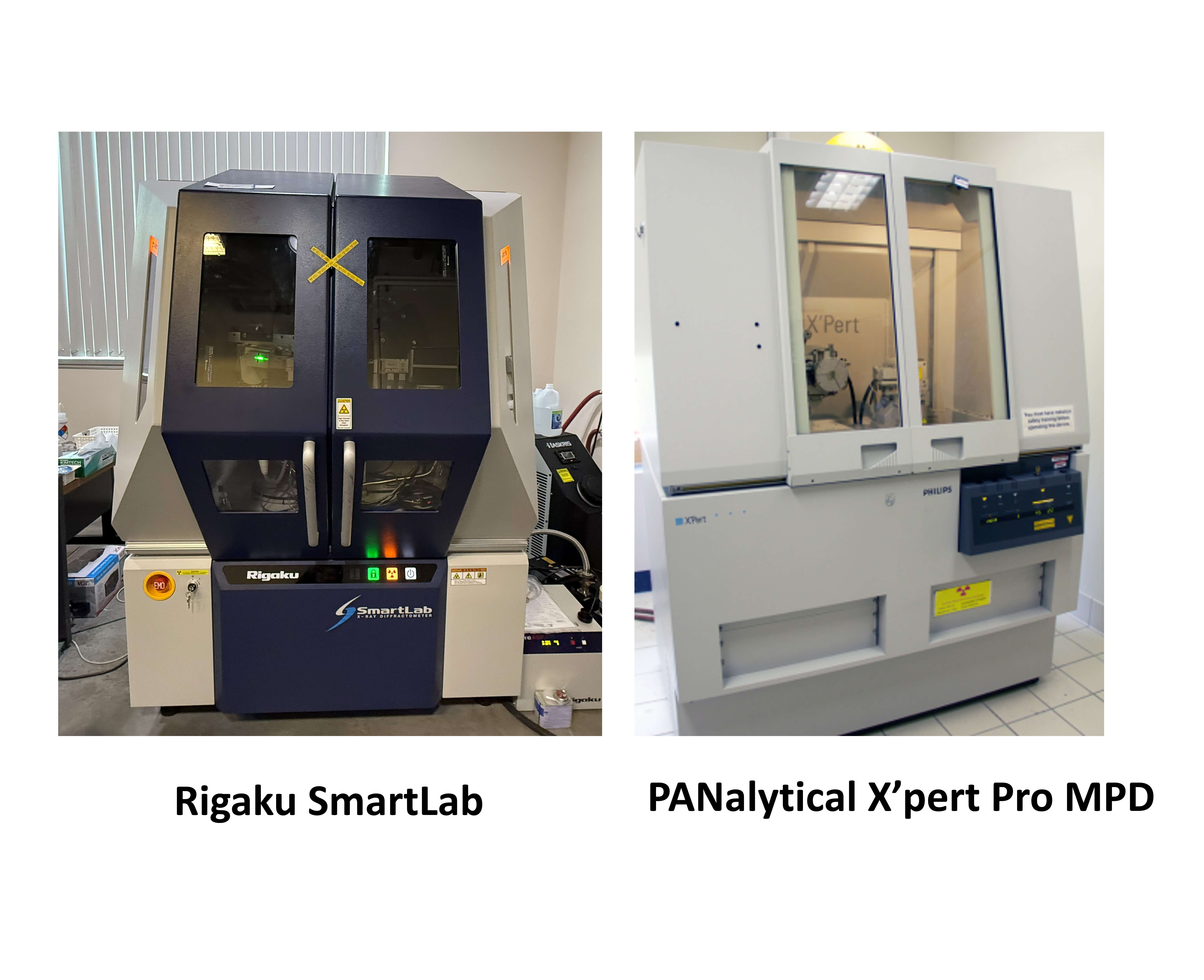
XRD
Research-grade X-ray diffraction systems including the Rigaku SmartLab and PANalytical X’Pert Pro MPD provide comprehensive structural characterization of crystalline materials. Capabilities include phase identification, crystal structure analysis, lattice parameter determination, residual stress measurement, texture characterization, thin-film analysis, and reciprocal space mapping.
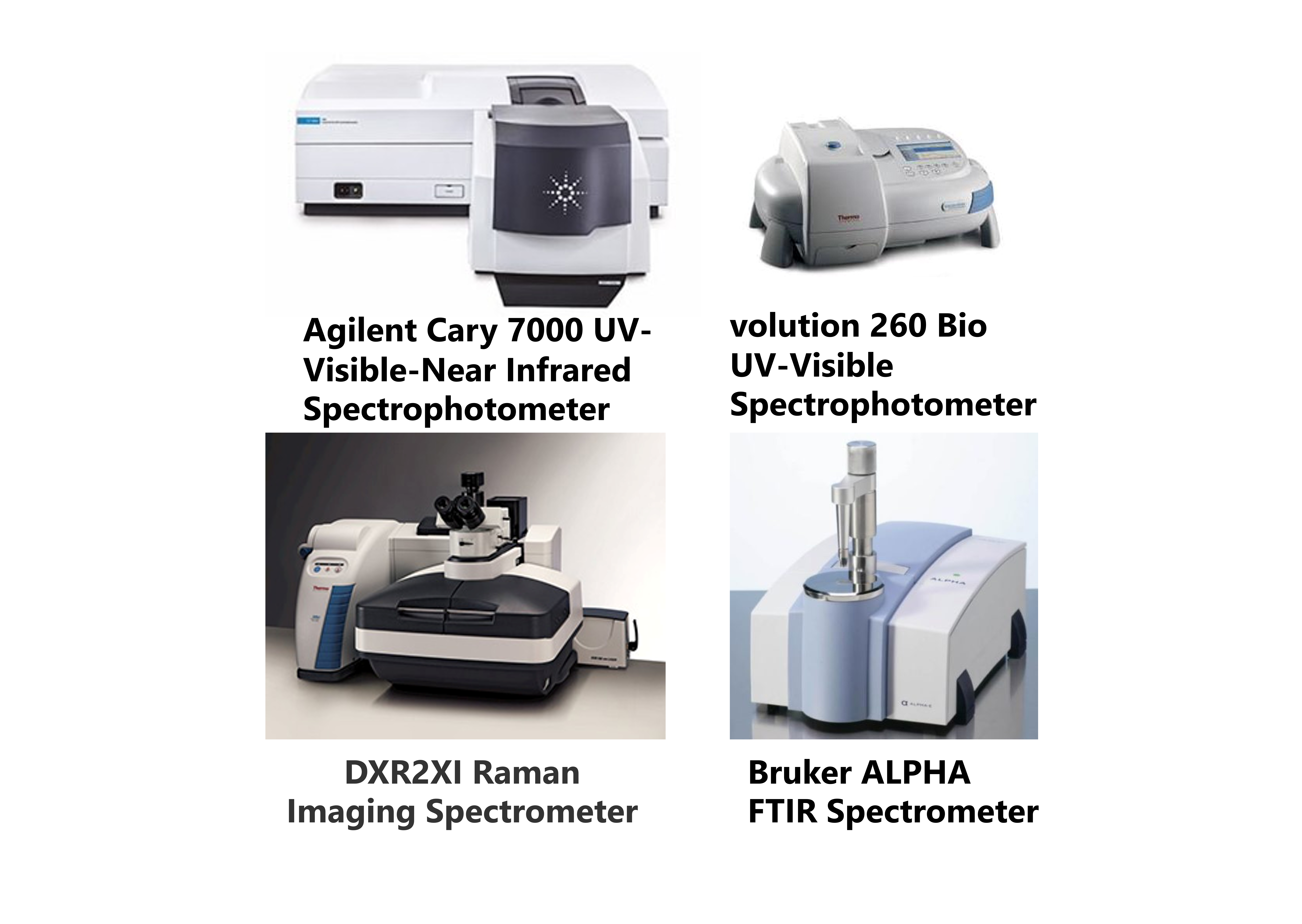
Optical & Vibrational Spectroscopy
Optical characterization using Raman, infrared, ultraviolet–visible, photoluminescence, and related spectroscopic techniques to probe crystal structure, composition, stress, and optical properties.
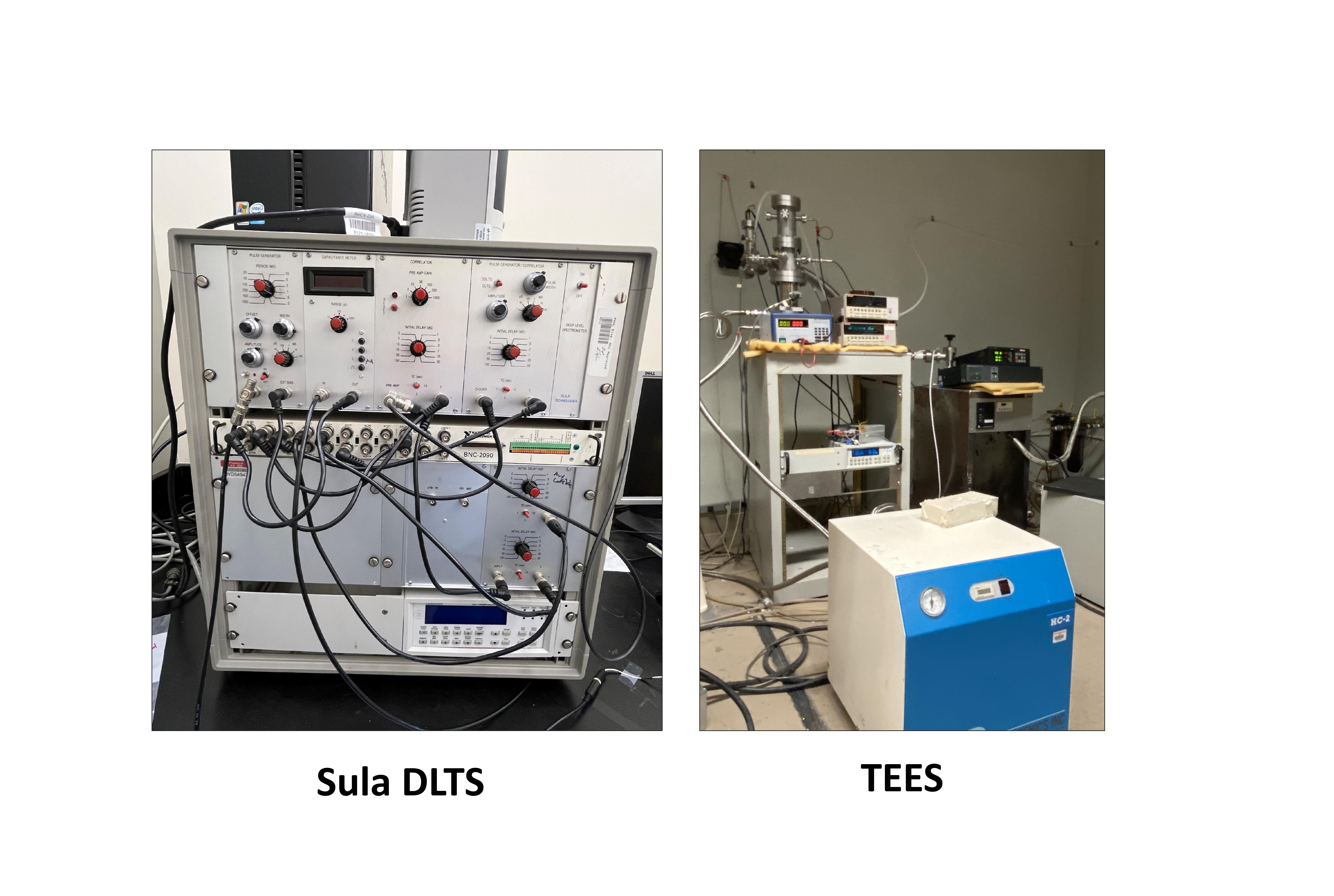
Electronic Defect Characterization
Advanced defect characterization using Positron Annihilation Spectroscopy (PAS), Thermally Stimulated Current/Thermally Stimulated Emission Spectroscopy (TSC/TEES), and Deep-Level Transient Spectroscopy (DLTS) to probe vacancy defects, deep-level states, carrier traps, and recombination mechanisms in semiconductor materials and devices.
Funding & Partners
- Over the years, IMR research has been supported through grants, contracts, and collaborative projects with federal agencies, national laboratories, universities, foundations, and industry partners.
- Funding and Collaborative Partners
- NSF · DOE · NNSA · ONR · DHS · DNDO · NIH
- NRL(NREL) · PNNL · LLNL
- TU Delft · Ghent University · UNICEN · UCLA · University of Utah
- W. M. Keck Foundation
- Dow · IBM · Intel · Boeing · Applied Materials · Cermet · II-VI · VLOC · eV Products · Honeywell · Novellus Systems · Radiation Detection Technologies · Outermost Technologies · Dow Corning · Bekaert
Contact
- Need a service:
- Rebecca Huffman (imr.orders@wsu.edu | rebecca.huffman@wsu.edu)
- Cooperation:
- Dave Field (dfield@wsu.edu)
- John McCloy (john.mccloy@wsu.edu)
- Location:
- Engineering Teaching and Research Laboratory (ETRL), 980 College Avenue, Washington State University, Pullman, WA 99164-2711.