WSU IMR has extensive single-crystal growth capabilities spanning II–VI and III–V semiconductors, oxide crystals, scintillators, laser crystals, and functional materials. Using the Travelling Heater Method (THM), High Pressure Bridgman (HPB), Modified Vertical Bridgman (MVB), Vertical Gradient Freeze (VGF), Accelerated Crucible Rotation Technique (ACRT), Czochralski (CZ), and Kyropoulos methods, we can grow crystals ranging from volatile compound semiconductors such as CdTe and CdZnTe to high-temperature oxides such as YAG, Ga₂O₃, sapphire, and ruby.
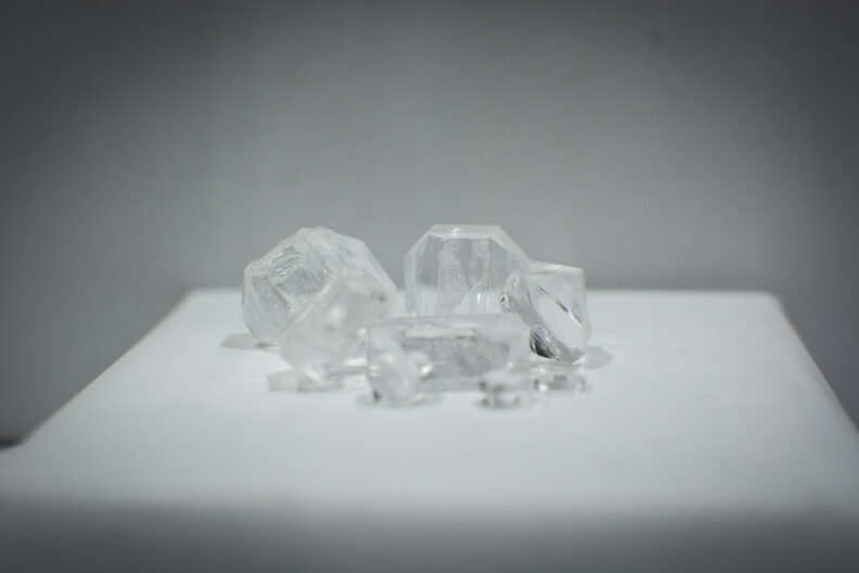
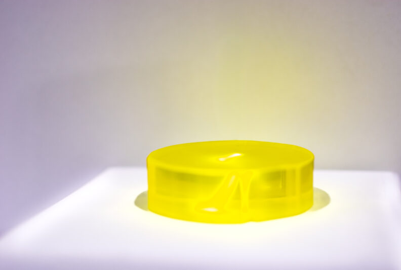
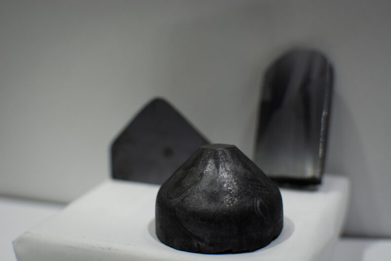
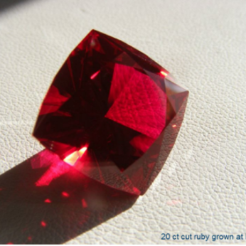
Crystals grown in IMR
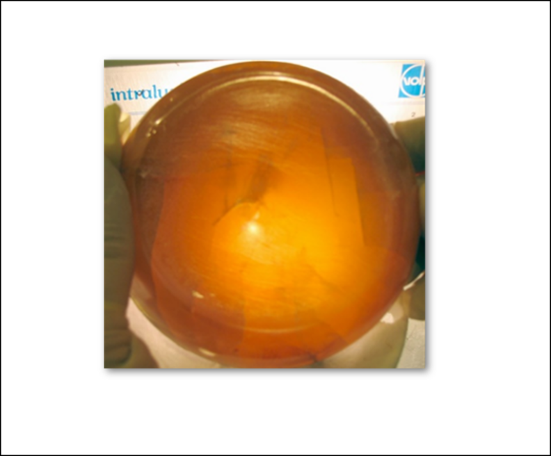
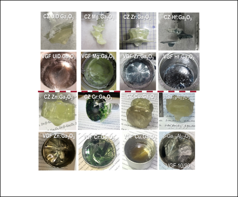
Crystal Growth Capabilities at WSU
At WSU, we operate a comprehensive suite of crystal-growth systems, including two multi-zone Modified Vertical Bridgman (MVB) furnaces, a custom-built four-zone Travelling Heater Method (THM) furnace, a High Pressure Bridgman (HPB) furnace, and a Czochralski (CZ) furnace. The CZ system can also be configured for Vertical Gradient Freeze (VGF) and Kyropoulos growth and includes controlled crucible rotation.
Each furnace is equipped with dedicated power, control, and monitoring systems. LabVIEW® software and National Instruments® hardware are used for customized process control, real-time monitoring, and recording of temperature profiles and other growth parameters.
Over the past three decades, these facilities have supported extensive research in semiconductor, optical, scintillator, piezoelectric, and wide-bandgap oxide single crystals. In addition to students working on CdTe and related materials, 10 PhD researchers have contributed to the growth, characterization, doping, and defect engineering of oxide and functional crystals:
- Jing Shang, “Optimization of N-Type CdTe and Cd-Se-Te for Next-Generation Solar Cells”, PhD 2025, Materials Science & Engineering.
- Benjamin L. Dutton, “Growth and Characterization of Ultrawide-Bandgap Oxide Semiconductors,” PhD 2025, Materials Science & Engineering.
- Jani Jesenovec, “Doping and Alloying of Monoclinic β-Ga₂O₃ Grown by Czochralski and Vertical Gradient Freeze,” PhD 2022, Materials Science & Engineering.
- Muad Saleh, “Characterization and Optimization of Dopants, Impurities, and Defects in Bulk Optical and Semiconductor Materials: Case Studies on ZnS, β-Ga₂O₃, and Nd:YAG,” PhD 2019, Materials Science & Engineering.
- Peter Dickens, “Atomic Defects of Czochralski-Grown Cerium and Calcium Co-Doped Yttrium Aluminum Garnet, Cerium and Lithium Co-Doped Yttrium Aluminum Garnet, and Rare-Earth-Doped Lithium Aluminate,” PhD 2016, Materials Science & Engineering.
- Drew Haven, “Activator Efficiency of Cerium-Doped Yttrium Aluminum Garnet by Defect Engineering,” PhD 2013, Materials Science & Engineering.
- Narendra Parmar, “Intrinsic Defects and Sodium Acceptor Doping in Zinc Oxide,” PhD 2012, Physics.
- Denis Solodovnikov, “Improving Scintillation Performance of Ce-Doped Garnet Crystals by Defect Engineering,” PhD 2010, Physics.
- Romit Dhar, “Growth and Optimization of Piezoelectric Single-Crystal Transducers for Energy Harvesting from Acoustic Sources,” PhD 2009, Materials Science & Engineering.
- Charles Shawley, “Optical and Defect Studies of Wide-Band-Gap Materials,” PhD 2008, Materials Science & Engineering.
From 1996 to 2026, our laboratories have grown at least 16 distinct crystal compositions, excluding dopant and alloying variations. These materials span II–VI and III–V semiconductors, ultrawide-bandgap oxides, laser and scintillator crystals, and piezoelectric and nonlinear optical materials.
| Crystal / Material Family | Number of Growths | Growth Method | Dopants / Composition |
| CdTe-based Semiconductors — CdZnTe (CZT), CdSeTe (CST), CdTe | >300 | CZT: VB, THM, CZ; CST: VB; CdTe: VB, THM, HPB | CZT: Er, Dy, V, Fe, Pb, Ge, Bi, In, Al; CST: As, In; CdTe: P, As, Sb, In, Cl, I |
| Related II–VI Semiconductors — CdSe, ZnTe, ZnSe | ~10 | HPB / Bridgman | — |
| Tellurium Oxides — CdTe₂O₅, CdTeO₃, ZnTeO₃, Zn₂Te₃O₈ | ~10 | VB, CZ | — |
| Piezoelectric / Ferroelectric Perovskites — PMN-PT; (Ba,Sr)TiO₃ (BST) | >20 PMN-PT; 4 BST | HPB; VGF | PMN-PT: x = 0.30, 0.32 |
| III–V Semiconductor — GaAs | ~10 | VB | — |
| Garnet / Scintillator Crystals — YAG, GGG, mixed garnets, Cs₂LiCeCl₆ | >60 garnets; ~5 elpasolite | CZ, VGF; VB | YAG: Ce, Er, Yb, Nd, B, Li, Ca; GGG: Ce, Tb |
| Wide-Bandgap / Optical Oxides — Ga₂O₃, LiAlO₂, Ruby/Sapphire, Bi₂WO₆, Gd₂GeO₅ | >70 Ga₂O₃; >20 LiAlO₂; ~10 Al₂O₃; ~5 each Bi₂WO₆/Gd₂GeO₅ | CZ, VGF | Ga₂O₃: Ca, Mg, Zr, Hf, Al, Cr, Zn, Cu, Mn, Sc, In; LiAlO₂: Mg, Ti, Ca, Ce, Eu, Pr; Al₂O₃: Cr, Ti, Fe |
| Nonlinear Optical Crystal — KDP (KH₂PO₄) | ~10 | Solution growth* | — |