Positron Annihilation Spectrometer
For further information please contact Marc Weber at (509) 335-8145 or cleanroom.imr@wsu.edu
Positron annihilation spectroscopy (PAS) techniques are a powerful means to detect vacancy and vacancy-related defects and defect complexes. The size of the open-volume defects and the chemical type of nearest neighbors can be identified. Depth resolved information is obtained with a mono-energetic variable energy beam. IMR is home to a 0 to 70 keV monoenergetic beam able to probe from the surface to 10 to 20 micrometers depth (density dependent) with a sensitivity from 10-7 to 10-3 per atom. Available PAS techniques include standard Doppler Broadening, coincident-Dopper broadening, Positronium detection and beam based lifetime measurements. A large body of positron annihilation spectroscopy research has been conducted on many materials at WSU.
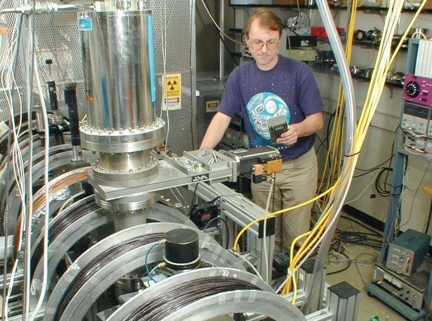
WSU’s Variable Energy Positron Beam Materials Characterization System is used for profiling open-volume defects in materials. Incident positron energies at the sample can be varied from 0.01 keV to 70 keV which corresponds to mean implantation depth up to 15 µm in Si and 6 µm in CdTe. Implantation depth in other materials scale with density (a higher density lowers the mean depth). Data can be collected at 2 primary experimental stations, a 2 detector Doppler broadening station and a lifetime station (pending a higher beam intensity).
The PAS capabilities are available as part of the IMR service center.
- Doppler broadening: Samples can be exposed to the implantation energy range at temperatures from 10 K to about 1300 K as well as while being illuminated by light from a variety of sources. Two high purity high efficiency Ge detectors and 1.4 keV full width at half maximum energy resolution at 511 keV. They are operated either independently or in coincidence for implantation depth profiles and standard (S and W) measurements as well as to determine surface properties via the formation of Positronium (a hydrogen atom-like bound state of a positron and an electron). The latter is used for porosity characterization, the former for vacancy and vacancy cluster characterization. Depth profiles allow for the extraction of diffusion lengths which in turn are used to calculate defect concentrations.
- Positron lifetime system: The same beam can be directed at samples. The lifetime resolution is about 400 ps depending on whether time resolution is important (vacancies and other point defects) or signal rate and large nanometer diameter pores are to be examined. Depth profiles to several micrometer depth can be obtained. Secondary electrons from positrons incident on the sample are detected with a channel electron multiplier array (CEMA) to provide the time-start pulse. Positron annihilation gamma rays are picked up by a fast CsF (or CeBr3 or BaF2) scintillator for the time-stop. Time spectra can be recorded in a up to 65 000 channel array to span over 1 microsecond with sub 10ps/channel resolution. The simultaneous lifetime fitting for <200ps of free and trapped positrons to 142 ns is possible (the lifetime of ortho-positronium in vacuum). This system is unique in the United States. No other lifetime system can be optimized to probe layers at several micrometer depth and down to nm near surface regions.
- In situ work can be carried out as a function of temperature (up to 1000°C), illumination or electric fields.
WSU’s positron beam was developed from the experiences of developing, building and operating over 8 positron beams by Kelvin Lynn and his team. Materials and research questions addressed at WSU include:
Annihilation in flight, three photon annihilations of free positrons, quantum confinement in CdSe quantum dots, vacancy defects in amorphous silicon for solar cells, SiC, SiGe, GaN, GaAs, ZnO, Ga2O3, YAG, CdTe and CdZnTe, ceramics, aluminum, palladium, uranium and its oxide, superconducting Nb, porous low-k dielectric films, leached glasses for nuclear waste storage, porous silicon, and vacancy formation enthalpies. Current work focuses on perovskite based solar cell materials and Ga2O3 single crystals.
Laboratory: Webster 547