SOLAR ENERGY
Projects
“Study of electro-optical properties in single crystal CdSeTe with varying Se and group V doping” (2024-2026) – McCloy
Funding: Cadmium Telluride Accelerator Consortium, National Renewable Energy Lab
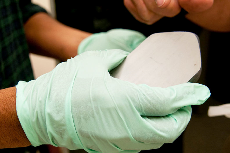
Washington State University aims to provide fundamental knowledge to improve efficiency of CdSeTe-based thin film solar cells. CdSeTe, with up to 40% tellurium replaced by selenium, shows promise for large-scale production, but the open circuit voltage (Voc) remains below the theoretical limit, hindering cell performance. The study will systematically investigate the role of selenium and p-type dopants in CdSeTe on properties using single crystal growth. Key tasks include growing crystals with varying Se composition (0, 10, 20, 40% Se) and group V dopants (P, As, Sb, Bi) and performing detailed material characterization. The goal is to understand the factors that reduce Voc and find ways to mitigate them, ultimately improving the solar cell’s efficiency.
“Optimizing Iodine-doped CdTe for Potential n-type Solar Cells” (2023-2025) – McCloy
Funding: Cadmium Telluride Accelerator Consortium, National Renewable Energy Lab
Washington State University will develop CdTe homojunctions using iodine doped n-type CdTe absorbers that are shown to have high carrier concentration and minority carrier lifetime with 100% dopant activation. We will apply a combination of defect spectroscopy techniques, optimize surface passivation techniques, and device architecture, and aim to overcome present performance limitations based on p-type absorber.
“Commercial Production of the Group-V Doped Polycrystalline CdTe Source Material for the Next-Generation Photovoltaic” (2022-2023, Phase I; 2023-2024, Phase 2) – McCloy
Funding: Department of Energy, Small Business Technology Transfer (STTR)
Partners: Radiation Detection Technologies (RDT), Colorado State University
The proposed technology transfer will allow for the mass production of crucial materials for the domestic solar industry that is not commercially available at the moment. These doped CdTe materials have the potential to improve the current CdTe photovoltaic efficiency and cell lifetime. The success of this effort will likely disrupt the current thin film solar energy supply chain.
“Developing CdTe homojunctions applying high throughput deposition” (2021-2022) – McCloy, Swain
Funding: Department of Energy – Office of Energy Efficiency & Renewable Energy – Solar Energy Technology Office, Small Innovative Projects in Solar
Partners: National Renewable Energy Laboratory
In order to fabricate homojunctions, we will develop indium (In) and iodine (I)-doped n-type CdTe that is compatible with a GrV-doped p-type CdTe absorber. In this project, we will design, fabricate, and study CdTe homojunctions, combining modeling, bulk and thin film growth of doped CdTe, and material and device characterization. The junction will be made by depositing highly n-type epitaxial films on p-type single crystal substrates. A fast close-space sublimation epitaxy (CSSE) process, which has been shown to produce single crystal films, will be used to make n-type films by in-situ doping. As source material, pre-doped CdTe:In and CdTe:I materials, grown by the Bridgman method, will be used. Device modeling will be performed, which will guide desired optimization of material properties and device design for making efficient junctions.
News: Department of Energy grant aims for more efficient solar technology
“Developing a low cost, high volume and scalable manufacturing technology for undoped and heavily p-type doped CdTe feedstock materials” (2016-2021) – Lynn, McCloy
Funding: Department of Energy – Office of Energy Efficiency & Renewable Energy – Solar Energy Technology Office – Photovoltaics Research & Development
Partners: National Renewable Energy Laboratory, Nious Technologies
WSU Insider Article: Researchers Advance Solar Material Production
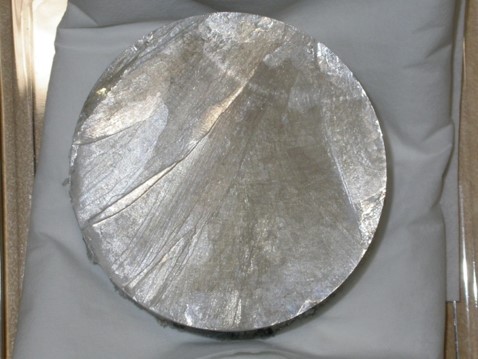
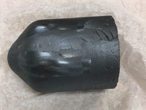
The goal is to establish a cost effective and scalable production approach of feedstock (CdTe and CdSeTe) for the solar industry, with the material properties necessary to improve performance and reduce costs. The primary focus is to develop a CdTe synthesis and growth process that pushes the p-type doping of CdTe to previously unattainable levels, while creating a path to scalable production. Based on previous results, we will aggressively explore how to effectively incorporate the p-type dopant during crystal growth. In our approach, the first step will be bulk CdTe growth doped with phosphorus using the Modified Vertical Bridgman (MVB) and high Pressure Bridgman (HPB) technique, and the second step will examine films deposited by Close-Spaced Sublimation (CSS) and Vapor Transport Deposition (VTD) using specialized feedstock. Systematic defect spectroscopy will be conducted to characterize the point and extended defect distribution.
“Preparation and evaluation of n-type CdSeTe as an absorber in thin film CdTe PV” (2019-2020) – Lynn, Swain
Funding: Department of Energy – Office of Energy Efficiency & Renewable Energy – Solar Energy Technology Office – Small Innovative Projects in Solar
Partners: National Renewable Energy Laboratory
In the present effort we will investigate the doping efficiency of n-type CdTe and CdSeTe as potential absorber materials for thin film PV application. Initially melt growth of CdTe and CdSeTe bulk crystals doped with indium will be performed by vertical Bridgman method. The electrical property and activation of dopants in single crystals will be measured by Hall effect after determining the dopant concentration by ICP-MS. Post growth treatment of single crystals under overpressure conditions will be performed to better understand the activation. Thin films will be fabricated from the CdTe:In and CdSeTe:In targets by RF magnetron sputtering, on CdTe single crystals and other appropriate substrates.
Publications
WSU Authors in bold, most recent first
Publications 2021-2025
- Jing Shang, Magesh Murugesan, Rubi Gul, Samuel Bigbee-Hansen, Joseph M. Tallan, Joel N. Duenow, John S. McCloy, “Structural and Electronic Properties of Indium-Doped n-type Cd-Se-Te Crystals for Solar Cells,” Journal of Electronic Materials, 53(7), 3848-3860. https://doi.org/10.1007/s11664-024-11094-w
- M. Murugesan, S. Swain, and J. McCloy, “Investigation of Electro-Optical Properties of Cadmium Selenide (CdSe) Single Crystals: Impact of Annealing in Selenium (Se) Vapor,” Proc. 2024 IEEE 52nd Photovoltaic Specialist Conference (PVSC), 1166-1168 (2024). http://dx.doi.org/10.1109/PVSC57443.2024.10749104
- J. Shang, J.N. Duenow, S.W. Johnston, H.R. Moutinho, M. Murugesan, and J.S. McCloy, “Characterization of n-Type Iodine-Doped and Indium-Doped CdTe/Cd-Se-Te Thin Films Fabricated by Close-Spaced Sublimation Epitaxy,” Proc. 2024 IEEE 52nd Photovoltaic Specialist Conference (PVSC), 1523-1531 (2024). http://dx.doi.org/10.1109/PVSC57443.2024.10749310
- B. Montag, A. Munshi, S. Walajabad, S. Swain, J. McCloy, and C. Rietcheck, “Commercial Production of the Group-V Doped Polycrystalline CdTe Source Material for the Next-Generation Photovoltaics,” Proc. 2024 IEEE 52nd Photovoltaic Specialist Conference (PVSC), 1-1 (2024). https://doi.org/10.1109/PVSC57443.2024.10749023
- Danielson, A., C. Reich, R. Pandey, A. Munshi, A. Onno, W. Weigand, D. Kuciauskas, S. Li, A. Bothwell, J. Guo, M. Murugesan, J.S. McCloy, R. Klie, Z.C. Holman, and W. Sampath, “Electro-optical characterization of arsenic-doped CdSeTe and CdTe solar cell absorbers doped in-situ during close space sublimation,” Solar Energy Materials and Solar Cells, 251, 112110 (2023). https://doi.org/10.1016/j.solmat.2022.112110
- J. Shang, M. Murugesan, S. Bigbee-Hansen, S.K. Swain, J.N. Duenow, S. Johnston, S.P. Beckman, H.H. Walker, R.W. Antonio, and J.S. McCloy, “The effect of dopant concentration and annealing treatments on N-type Iodine doped CdTe,” Journal of Alloys and Compounds, 960, 170625 (2023). https://doi.org/10.1016/j.jallcom.2023.170625
- J Shang, M Murugesan, R Gul, S Bigbee-Hansen, J M Tallan, J N Duenow, J S McCloy, “Structural and Electronic Properties of Indium-Doped n-type Cd-Se-Te Crystals for Solar Cells,” Journal of Electronic Materials, accepted, (2024). https://doi.org/10.1007/s11664-024-11094-w
- Nagaoka, S. K. Swain and A. H. Munshi, “Review on Group-V Doping in CdTe for Photovoltaic Application,” IEEE Journal of Photovoltaics, 14(3), 397-413, (2024). https://doi.org/10.1109/JPHOTOV.2024.337408
Publications 2019-2020
- Munshi, A.H., A.H. Danielson, S. Swain, C.L. Reich, T.M. Shimpi, S.W. McPherson, K.G. Lynn, D. Kuciauskas, A. Ferguson, J. Guo, R. Klie, and W.S. Sampath, “Doping CdSexTe1-x/CdTe Graded Absorber Films with Arsenic for Thin-Film Photovoltaics,” Proc. 2019 IEEE 46th Photovoltaic Specialists Conference (PVSC), 28-31 (2019). https://doi.org/10.1109/PVSC40753.2019.8980634
- S. K. Swain, J.N. Duenow, S.W. Johnston, M. Amarasinghe, J.J. McCoy, W.K. Metzger, and K.G. Lynn, “Approach to Defect-Free Lifetime and High Electron Density in CdTe,” Journal of Electronic Materials, 48(7), 4235-4239 (2019). https://doi.org/10.1007/s11664-019-07190-x
- Swain, S.K., Ablekim, and K.G. Lynn, “Defect Study of Group V Doped CdTe By Thermoelectric Effect Spectroscopy,” Proc. 2019 IEEE 46th Photovoltaic Specialists Conference (PVSC), 3063-3065 (2019). https://doi.org/10.1109/PVSC40753.2019.8980634
- Amarasinghe, M., E. Colegrove, D. Albin, S. Swain, J. Duenow, X. Zheng, A. Ferguson, K. Lynn, and W.K. Metzger, “Group-V dopant Incorporation for High CdSeTe/CdTe Hole Density and Lifetime,” Proc. 2019 IEEE 46th Photovoltaic Specialists Conference (PVSC), 0025-0027 (2019). https://doi.org/10.1109/PVSC40753.2019.8981177
- Guo, J., A. Sharma, A. Munshi, C. Reich, A. Danielson, W. Sampath, S. Swain, and R. Klie, “Study of Arsenic Doped CdSeTe Solar Cells Using Transmission Electron Microscopy,” Microscopy and Microanalysis, 26(S2), 1232-1234 (2020). https://doi.org/10.1017/S1431927620017420
- Munshi, A.H., C.L. Reich, A.H. Danielson, R. Pandey, D. Kuciauskas, J. Guo, S. Li, A. Shah, Swain, T.M. Shimpi, T.K. Al-Hamdi, K.G. Lynn, R.F. Klie, and W.S. Sampath, “Arsenic Doping of Polycrystalline CdSeTe Devices for Microsecond Life-times with High Carrier Concentrations,” Proc. 2020 47th IEEE Photovoltaic Specialists Conference (PVSC), 1824-1828 (2020). https://doi.org/10.1109/PVSC45281.2020.9301003
- McPherson, S.W., Al-Hamdi, J.N. Duenow, X. Zheng, D.S. Albin, T. Ablekim, E. Colegrove, M. Amarasinghe, W.K. Metzger, S.K. Swain, and K.G. Lynn, “Optimization of source material for in-situ Arsenic doping via vapor transport deposition of CdTe films,” Proc. 2020 47th IEEE Photovoltaic Specialists Conference (PVSC), 1913-1915 (2020). https://doi.org/10.1109/PVSC45281.2020.9300719
- Jamarkattel, M.K., A.B. Phillips, A. Quader, K.K. Subedi, F.K. Alfadhili, S.S. Bista, R.A. Awni, D.B. Li, S. K. Swain, Y. Yan, R.J. Ellingson, J.S. McCloy, K.G. Lynn, and M.J. Heben, “Incorporation of Arsenic in CdSe/CdTe Solar Cells During Close Spaced Sublimation of CdTe:As,” Proc. 2020 47th IEEE Photovoltaic Specialists Conference (PVSC), 2605-2608 (2020). http://www.doi.org/10.1109/PVSC45281.2020.9300772
- Al-Hamdi, T.K., S.W. McPherson, S.K. Swain, J. Jennings, J.N. Duenow, X. Zheng, D.S. Albin, T. Ablekim, E. Colegrove, M. Amarasinghe, A. Ferguson, W.K. Metzger, C. Szeles, and K.G. Lynn, “CdTe synthesis and crystal growth using the high-pressure Bridgman technique,” Journal of Crystal Growth, 534, 125466 (2020). https://doi.org/10.1016/j.jcrysgro.2019.125466
Publications 2016-2018
- Burst, J.M., J.N. Duenow, D.S. Albin, E. Colegrove, M.O. Reese, J.A. Aguiar, C.S. Jiang, M.K. Patel, M.M. Al-Jassim, D. Kuciauskas, S. Swain, T. Ablekim, K.G. Lynn, and W.K. Metzger, “CdTe solar cells with open-circuit voltage breaking the 1 V barrier,” Nature Energy, 1(3), 16015 (2016). https://doi.org/10.1038/nenergy.2016.15
- T. Ablekim, S. Swain, W.-J. Yin, K. Zaunbrecher, J. Burst, T. Barnes, D. Kuciauskas, S.-H. Wei, and K. Lynn, “Self-compensation in arsenic doping of CdTe,” Scientific Reports, 7, 4533 (2017). https://doi.org/10.1038/s41598-017-04719-0
- Perkins, C.L., T. Ablekim, T.M. Barnes, D. Kuciauskas, K. G. Lynn, W. Nemeth, M.O. Reese, S.K. Swain, and W.K. Metzger, “Interfaces Between CdTe and ALD Al2O3,” IEEE Journal of Photovoltaics, 8(6), 1858-1861 (2018). https://dx.doi.org/10.1109/JPHOTOV.2018.2870139
- Ščajev, P., S. Miasojedovas, A. Mekys, D. Kuciauskas, K. G. Lynn, S.K. Swain, and K. Jarašiūnas, “Excitation-dependent carrier lifetime and diffusion length in bulk CdTe determined by time-resolved optical pump-probe techniques,” Journal of Applied Physics, 123(2), 025704 (2018). https://doi.org/10.1063/1.5010780
- J. J. McCoy, K. Swain, J.R. Sieber, D.R. Diercks, B.P. Gorman, and K.G. Lynn, “p-type doping efficiency in CdTe: Influence of second phase formation,” Journal of Applied Physics, 123(16), 161579 (2018). https://doi.org/10.1063/1.5002144
- Danielson, A., A. Munshi, A. Kindvall, S. K. Swain, K. Barth, K. Lynn, and W. Sampath, “Doping CdTe Absorber Cells using Group V Elements,” Proc. 2018 IEEE 7th World Conference on Photovoltaic Energy Conversion (WCPEC) (A Joint Conference of 45th IEEE PVSC, 28th PVSEC & 34th EU PVSEC), 0119-0123 (2018). https://doi.org/10.1109/PVSC.2018.8547792